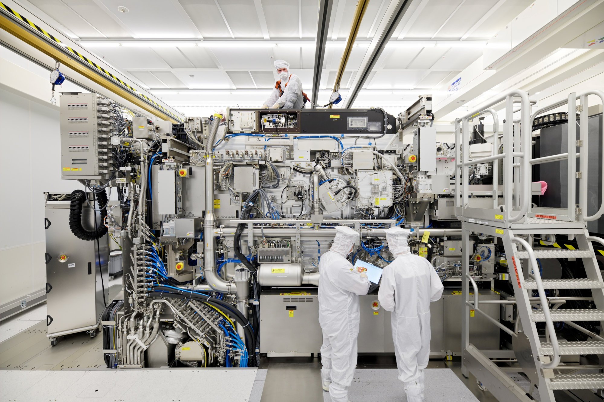
Even after China has spent years pursuing self-reliance in semiconductors, the lithography machines needed to make advanced chips today only come from one company: Netherlands-based ASML Holding. Producing this kind of complex machinery entirely within China is not likely to happen in the foreseeable future, industry insiders say.
Chinese chip makers can still access critical ASML equipment for four months
Chinese chip makers can still access critical ASML equipment for four months
Li Jinxiang, deputy secretary general of the China Electronic Production Equipment Industry Association, told a forum in August that no China-made lithographic machines are available for front-end chip-making, and developing domestic equipment will not be smooth sailing.
“We still have a long way to go in lithography (tools),” Li said at the time. “Not a single chip-making production line in China has equipped a China-made lithography system – most of them are only used in academic research.”
Both Huawei and SMIC have remained silent about the new Kirin processor since TechInsights published a report saying the chip was made by China’s largest foundry using improved techniques with existing equipment. US Commerce Secretary Gina Raimondo said last month that there is no evidence that China can produce 7-nm chips “at scale”, meaning the breakthrough may not lead to commercially viable mass production.
Before the Mate 60 Pro, Huawei’s last 5G smartphones, part of the Mate 40 series, were released in 2020.

Restricting access to advanced chip-making tools has been a key exploit for Washington to inflict pain on China’s domestic semiconductor industry. This includes working with the Netherlands and Japan to further restrict China-bound exports. Starting from January 2024, China will be cut off from buying ASML’s 2000-series immersion DUV lithography systems, threatening expansion plans for the country’s foundries.
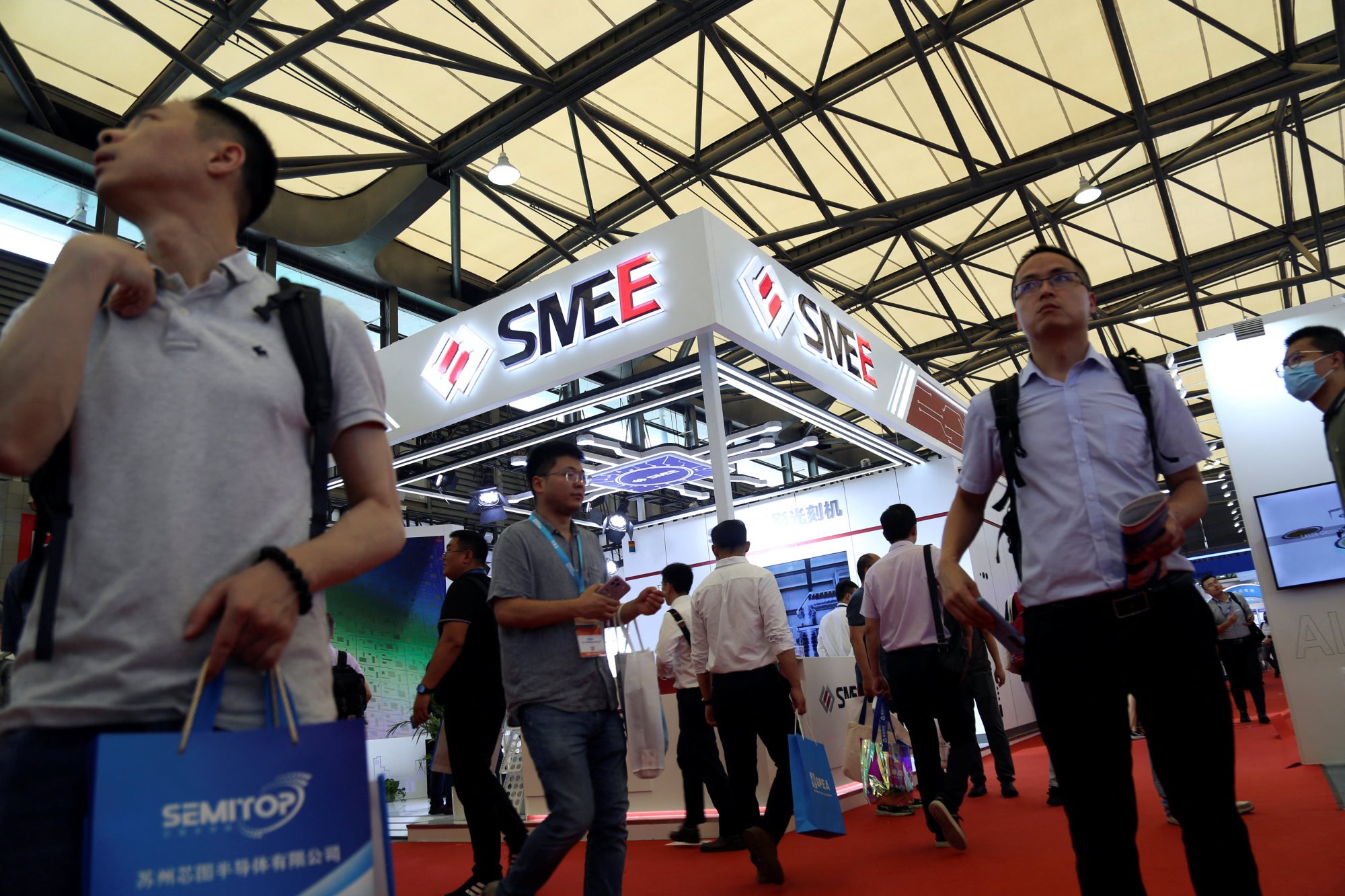
China has worked for years to develop its own lithography systems, pinning its hopes on the state-owned enterprise Shanghai Micro Electronics Equipment Group (SMEE). But the company’s best machine to date, the SSA600/20 scanner, is only capable of 90-nm lithography resolution, lagging far behind global peers such as AMSL and Japan’s Nikon.
It is not SMEE’s fault, as the company is handling “the hardest problem in the equipment field”, Zhu Yu, the founder of Beijing U-precision Tech, said at the 2023 Beijing Microelectronics International Symposium in Beijing on September 25, according to a speech transcript and presentation materials seen by the Post.
Chinese state-owned newspaper Securities Daily reported in August that SMEE may be able to deliver its first 28nm-capable lithography machine by the end of this year – an accomplishment that would be a breakthrough in Beijing’s drive for technological self sufficiency.
Overcoming restrictions on EUV machines will mean companies like SMEE need breakthroughs across multiple technologies including “light sources, advanced optics, and systems integration”, according to Paul Triolo, senior vice-president for China and technology policy lead at Albright Stonebridge Group.
“There are major efforts under way in China in the R&D phase to develop the key set of technologies critical to EUV lithography, but it will be at least four to five years before anything approaching a commercially capable system could be produced based only on Chinese suppliers,” Triolo said.
Jan-Peter Kleinhans, director of technology and geopolitics at Stiftung Neue Verantwortung (SNV), a Berlin-based think tank, said supply chains remain a major hurdle.
“SMEE is just not ‘there’ yet, and this is largely due to their suppliers,” he said. “To achieve [a domestically made immersion DUV system] they’d need hundreds, thousands of breakthroughs across SMEE’s entire supplier network consistently and concurrently.”

Lithography systems work by projecting special light through a pattern blueprint known as a “mask” or “reticle”, which then traverses the system’s optics designed to shrink and focus the pattern onto a photosensitive silicon wafer.
After the pattern is printed, the system moves the wafer slightly and makes another copy on the wafer. This process is repeated until the wafer is covered in patterns, completing one layer of the wafer’s chips. Making an entire microchip requires repeating this process layer after layer, stacking the patterns vertically to create an integrated circuit.
Stay connected with us on social media platform for instant update click here to join our Twitter, & Facebook
We are now on Telegram. Click here to join our channel (@TechiUpdate) and stay updated with the latest Technology headlines.
For all the latest Business News Click Here
